 Peter's electronic projects Peter's electronic projects
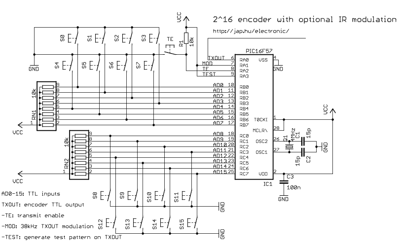
| pin |
name |
type |
description |
| 1 |
T0CKI |
TTL input |
connect to VDD |
| 2 |
VDD |
power |
connect to power supply |
| 3 |
NC |
not connected |
|
| 4 |
VSS |
power |
connect to ground |
| 5 |
NC |
not connected |
|
| 6 |
TXOUT |
TTL output |
transmit output. LOW when not
transmitting Connect directly to RF module DATA input pin for RF applications Connect to an IR LED directly or through a transistor for infrared applications** |
| 7 |
-MOD |
TTL input |
modulation - on powerup pull
HIGH to disable, pull LOW to enable 38kHz carrier |
| 8 |
-TE |
TTL input |
active low enable - pull LOW to
transmit |
| 9 |
-TEST |
TTL input |
active low enable - pull LOW on
powerup for generating a fixed test pattern |
| 10 |
AD0 |
TTL input |
address or data, optional active
low trigger* |
| 11 |
AD1 |
TTL input | address or data, optional active low trigger* |
| 12 |
AD2 |
TTL input |
address or data, optional active low trigger* |
| 13 |
AD3 |
TTL input |
address or data, optional active low trigger* |
| 14 |
AD4 |
TTL input |
address or data, optional active low trigger* |
| 15 |
AD5 |
TTL input | address or data, optional active low trigger* |
| 16 |
AD6 |
TTL input | address or data, optional active low trigger* |
| 17 |
AD7 |
TTL input | address or data, optional active low trigger* |
| 18 |
AD8 |
TTL input | address or data, optional active low trigger* |
| 19 |
AD9 |
TTL input | address or data, optional active low trigger* |
| 20 |
AD10 |
TTL input | address or data, optional active low trigger* |
| 21 |
AD11 |
TTL input | address or data, optional active low trigger* |
| 22 |
AD12 |
TTL input | address or data, optional active low trigger* |
| 23 |
AD13 |
TTL input | address or data, optional active low trigger* |
| 24 |
AD14 |
TTL input | address or data, optional active low trigger* |
| 25 |
AD15 |
TTL input | address or data, optional active low trigger* |
| 26 |
OSC2 |
XTAL output |
oscillator crystal output |
| 27 |
OSC1 |
XTAL input |
oscillator crystal input |
| 28 |
-MCLR |
ST input |
reset input, connect to VDD |
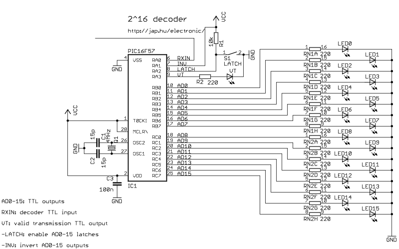
| pin |
name |
type |
description |
| 1 |
T0CKI |
TTL input |
connect to VDD |
| 2 |
VDD |
power |
connect to power supply |
| 3 |
NC |
not connected |
|
| 4 |
VSS |
power |
connect to ground |
| 5 |
NC |
not connected |
|
| 6 |
RXIN |
TTL input | receive input. Its polarity must
match the encoder output Connect directly to RF module DATA output pin for RF applications Connect to an IR receiver IC (eg. TSOP1738) output pin directly for infrared applications |
| 7 |
-INV |
TTL input |
active low - pull LOW to invert
AD0-AD15 outputs |
| 8 |
-LATCH |
TTL input |
active low - pull LOW to latch
last received data on AD0-AD15 pull HIGH to reset AD0-AD15 to default state on no reception |
| 9 |
VT |
TTL output |
valid transmission indicator -
HIGH when a valid packet is received LOW when there is no reception |
| 10 |
AD0 |
TTL input/output* |
address input or data output* |
| 11 |
AD1 |
TTL input/output* | address input or data output* |
| 12 |
AD2 |
TTL input/output* | address input or data output* |
| 13 |
AD3 |
TTL input/output* | address input or data output* |
| 14 |
AD4 |
TTL input/output* | address input or data output* |
| 15 |
AD5 |
TTL input/output* | address input or data output* |
| 16 |
AD6 |
TTL input/output* | address input or data output* |
| 17 |
AD7 |
TTL input/output* | address input or data output* |
| 18 |
AD8 |
TTL input/output* | address input or data output* |
| 19 |
AD9 |
TTL input/output* | address input or data output* |
| 20 |
AD10 |
TTL input/output* | address input or data output* |
| 21 |
AD11 |
TTL input/output* | address input or data output* |
| 22 |
AD12 |
TTL input/output* | address input or data output* |
| 23 |
AD13 |
TTL input/output* | address input or data output* |
| 24 |
AD14 |
TTL input/output* | address input or data output* |
| 25 |
AD15 |
TTL input/output* | address input or data output* |
| 26 |
OSC2 |
XTAL output |
oscillator crystal output |
| 27 |
OSC1 |
XTAL input |
oscillator crystal input |
| 28 |
-MCLR |
ST input |
reset input, connect to VDD |
| source
file |
line | meaning |
| enc-parallel.asm |
en_mask_portb
dt b'00000000' |
setup
AD7-AD0 bit triggers 0 sets trigger capability, 1 disables |
| enc-parallel.asm |
en_mask_portc dt b'00000000' |
setup AD15-AD8 bit triggers 0 sets trigger capability, 1 disables |
| dec-parallel.asm |
unimplemented |
select AD7-AD0 pins as address
bits 1 selects the pin as address input, 0 sets pin as data output |
| dec-parallel.asm |
unimplemented | select AD15-AD8 pins as address
bits 1 selects the pin as address input, 0 sets pin as data output |